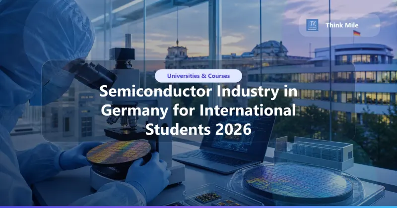
Semiconductor Industry in Germany for International Students 2026
Germany is betting billions on becoming Europe's semiconductor manufacturing hub. The EU Chips Act has designated Germany as a primary production site — with the ESMC joint-venture fab (TSMC, Bosch, Infineon, and NXP; over €10 billion combined investment) under construction in Dresden and Infineon's ongoing expansion in Munich and Dresden. For international students, this is a rare window: Germany is actively building the ecosystem and is structurally short on talent.
For Indian students with backgrounds in ECE, EE, Physics, or Materials Science, semiconductor programs in Germany offer something few countries can match: direct access to the companies building Europe's chip manufacturing capacity, thesis projects inside Infineon and TSMC Europe, and starting salaries in a sector paying €48,000–€68,000 for entry-level engineers, trending higher for chip-design roles. Ankit has personally guided 500+ Indian students to Germany across engineering programs, including students now in semiconductor and microelectronics roles.
💡 Find semiconductor and microelectronics programs matched to your background. Try the free AI University Finder — personalised results in 3 minutes.
Last reviewed: 21 September 2026. Semiconductor investment plans in Germany have shifted significantly — Intel permanently cancelled its planned €30 billion Magdeburg fab in July 2025, and EU Blue Card salary thresholds rise annually. Verify current fab timelines and Blue Card figures before relying on them for a career decision.
Germany's Semiconductor Sector in 2026
Germany is not just a chip buyer — it is becoming a chip maker. The EU Chips Act (2023) committed €43 billion to the EU semiconductor sector, with Germany receiving the largest share. Key developments:
| Company | Location | Investment | What they're building |
|---|---|---|---|
| ESMC (TSMC/Bosch/Infineon/NXP joint venture) | Dresden | €10 billion+ (combined) | Specialty chip fab; equipment move-in during 2026, production targeted late 2027 |
| Infineon | Munich / Dresden | €5 billion+ | Power semiconductors, automotive chips |
| Bosch | Dresden | €3 billion | Automotive semiconductors |
| GlobalFoundries | Dresden | Ongoing expansion | Specialty logic fabs |
Swipe horizontally to see more
Dresden is Germany's — and arguably Europe's — semiconductor capital. "Silicon Saxony" (the Dresden semiconductor cluster) already employs 80,000 people in the semiconductor supply chain and is expected to add further jobs as the ESMC fab ramps toward production.
Note that Intel's previously announced €30 billion Magdeburg fab — often cited in earlier coverage of Germany's semiconductor push — was permanently cancelled in July 2025 after Intel paused it in 2024 citing insufficient committed demand. It is not part of Germany's current semiconductor buildout; Intel still operates other Germany-based teams, but not a Magdeburg fab.
Munich is the home of Infineon (€15 billion revenue, 60,000+ employees) and the centre of Germany's power semiconductor and automotive chip design ecosystem.
For the broader context on studying engineering in Germany, see why Germany is the top choice for studying abroad.
Relevant Programs for Semiconductor Careers
Semiconductor careers in Germany require different academic backgrounds depending on the role:
| Career Path | Ideal Academic Background |
|---|---|
| Chip design / IC design | EE, ECE, Microelectronics |
| Process engineering (fab) | Materials Science, Physics, Chemical Engineering, EE |
| Embedded firmware for ICs | ECE, CS (embedded systems) |
| Semiconductor equipment | Mechanical Engineering, Physics, EE |
| Power semiconductors | EE (power electronics focus) |
| Photonics / Laser (TRUMPF, Zeiss) | Physics, Optical Engineering |
| Test and characterisation | EE, Physics |
Swipe horizontally to see more
Key Program Types to Search For
- M.Sc. Microelectronics or Nanoelectronics
- M.Sc. Electrical Engineering (semiconductor devices focus)
- M.Sc. Nanostructure Technology
- M.Sc. Materials Science (electronic materials)
- M.Sc. Photonics / Optical Technologies
- M.Sc. Semiconductor Technology
Top Universities for Semiconductor Programs
1. Technical University of Munich (TUM) — Munich
Relevant Programs: M.Sc. Electrical Engineering and Information Technology (semiconductor devices, microsystems) / M.Sc. Physics (condensed matter / semiconductor physics)
TUM has strong semiconductor physics and device research in close proximity to Infineon's global headquarters (10 km away in Neubiberg). The EI program covers semiconductor device physics, VLSI design, and microsystems technology. Infineon and Intel Germany both have active partnerships with TUM.
| Detail | Info |
|---|---|
| Language | English + German |
| Duration | 2 years |
| Application deadline | 31 May (winter) |
| CGPA (indicative) | 8.0+ / 10 |
| Tuition | ~€144/semester |
| APS required | Yes |
Swipe horizontally to see more
2. Friedrich-Alexander University Erlangen-Nuremberg (FAU) — Erlangen
Relevant Programs: M.Sc. Nanostructure Technology (English-taught) / M.Sc. Advanced Optical Technologies / M.Sc. Electrical Engineering (microelectronics track)
FAU's Nanostructure Technology program is one of the few explicitly semiconductor-focused graduate programs in Germany. The program covers device physics, nano-fabrication, characterisation, and materials for semiconductors. FAU runs the Zentrum für Nanoanalytik und Technologietransfer (ZnT) — a clean room facility available to Master's thesis students.
| Detail | Info |
|---|---|
| Language | English-taught (Nanostructure Technology) |
| Duration | 2 years |
| Application deadline | 31 May (winter) |
| CGPA (indicative) | 7.0–7.5 / 10 |
| Tuition | ~€70/semester |
| APS required | Yes |
Swipe horizontally to see more
FAU has an exceptional semiconductor program-to-cost ratio: English-taught, directly relevant to Infineon (Erlangen campus), and one of the lowest semester fees in Germany. For Indian students specifically targeting semiconductor careers, FAU deserves strong consideration alongside TUM.
3. TU Dresden — Dresden
Relevant Programs: M.Sc. Micro and Nano Electronics (English-taught) / M.Sc. Materials Science / M.Sc. Physics (semiconductor devices)
Dresden is the most strategically placed university for semiconductor careers. TU Dresden's Center for Advancing Electronics Dresden (cfaed) is an excellence cluster focused on microelectronics innovation. The university has formal partnerships with TSMC Europe (ESMC), GlobalFoundries, and Infineon Dresden — thesis and internship pipelines that exist nowhere else in Germany.
| Detail | Info |
|---|---|
| Language | English programs available (Micro and Nano Electronics) |
| Duration | 2 years |
| Application deadline | 15 June |
| CGPA (indicative) | 7.5–8.0 / 10 |
| Tuition | ~€300/semester |
| APS required | Yes |
Swipe horizontally to see more
For students specifically targeting TSMC, GlobalFoundries, or Infineon Dresden, TU Dresden is the most logical university choice — the geographic and institutional proximity is unmatched.
4. University of Stuttgart — Stuttgart
Relevant Programs: M.Sc. Electrical Engineering (microsystems/MEMS focus) / M.Sc. Materials Science
Stuttgart's EE and materials science programs have strong MEMS (microelectromechanical systems) and semiconductor packaging research. The Institute for Micro Integration (IFM) does semiconductor packaging and microsystems research with direct industry partners in the Stuttgart–Munich corridor.
| Detail | Info |
|---|---|
| Language | Mixed (English + German) |
| Duration | 2 years |
| Application deadline | 30 April |
| CGPA (indicative) | 7.5+ / 10 |
| Tuition | ~€1,500/semester (non-EU fee) |
| APS required | Yes |
Swipe horizontally to see more
5. RWTH Aachen — Aachen
Relevant Programs: M.Sc. Electrical Engineering (microelectronics / semiconductor devices track) / M.Sc. Materials Engineering
RWTH Aachen's AMO GmbH (Advanced Microelectronic and Optoelectronic Research Center) collaborates with the university on nano-semiconductor research. While Aachen is not in Dresden's semiconductor cluster, it has connections to IMEC (Belgium, 45 km away) and Intel's European research centres.
| Detail | Info |
|---|---|
| Language | English programs available |
| Duration | 2 years |
| Application deadline | 15 June |
| CGPA (indicative) | 7.5+ / 10 |
| Tuition | ~€200/semester |
| APS required | Yes |
Swipe horizontally to see more
EU Chips Act: What It Means for International Students in 2026
The EU Chips Act has created a structural funding environment that directly benefits students and researchers:
Research Funding
The Chips Act includes €3.3 billion for R&D and innovation. German universities (particularly TU Dresden, TUM, and FAU) are receiving grants to expand semiconductor research — creating more Master's thesis positions and PhD studentships.
Job Creation
The ESMC Dresden fab (TSMC, Bosch, Infineon, NXP) will require thousands of process, equipment, and design engineers as it ramps toward its targeted late-2027 production start. Many of these roles will be filled by graduates coming from German university programs.
Internship and Thesis Opportunities
TSMC Europe (Dresden) and the ESMC partners have student programs with internship and thesis positions. Intel Germany's other operations also run university partnerships, though its planned Magdeburg fab was cancelled in 2025 and is no longer a hiring driver.
Immigration Advantage
Germany's Blue Card allows highly skilled non-EU graduates with a qualifying job offer to stay and work. The 2026 gross salary threshold is €50,700/year standard, or €45,934/year for shortage occupations, recent graduates, and qualifying IT specialists (thresholds rise most years — verify the current figure before relying on it). Most semiconductor engineering roles qualify at least under the reduced threshold. The 18-month Job Seeker Visa after graduation gives you extensive time to secure a position.
Key Semiconductor Companies in Germany for Students
Infineon Technologies (Munich / Dresden / Neubiberg)
Germany's largest semiconductor company. Manufactures power semiconductors, automotive chips, and security ICs. Actively hires Master's thesis students from TUM, FAU, and TU Dresden.
TRUMPF (Ditzingen, near Stuttgart)
World leader in industrial lasers and laser-based chip manufacturing systems (EUV laser technology). Laser physics and optical engineering backgrounds are directly relevant.
Carl Zeiss (Oberkochen)
Makes the optical systems used in ASML's EUV lithography machines — which manufacture every advanced chip in the world. Optics, photonics, and precision engineering programs at FAU, Stuttgart, and Jena University are the primary pipelines.
Bosch Semiconductor (Reutlingen / Dresden)
Bosch invested €3 billion in a semiconductor fab in Dresden, focused on automotive chips (300mm wafers). Strong demand for process engineers and device engineers.
GlobalFoundries (Dresden)
Specialty logic foundry. Hires from TU Dresden's engineering and materials science programs for process engineering and equipment roles.
Aixtron (Aachen)
Makes MOCVD equipment used in compound semiconductor and LED manufacturing. Strong connection to RWTH Aachen's materials and EE programs.
💡 Ready to position yourself for Germany's semiconductor hiring wave? Chat with Ankit about your application strategy — Mentor Pack at ₹29,999. Package validity: One target intake or up to one year from the joining date, whichever comes first, with SOP review and university shortlist guidance.
Admission Requirements for International Students
Eligible Academic Backgrounds
| Background | Suitable for | Notes |
|---|---|---|
| ECE / EE | IC design, device physics, embedded for ICs | Direct match |
| Physics | Semiconductor device physics, photonics, fab process | Strong match |
| Materials Science / Engineering | Process engineering, fab, packaging | Direct match |
| Chemical Engineering | Semiconductor process (CVD, etch, clean processes) | Good match |
| Mechanical Engineering | Equipment engineering, MEMS | Moderate match |
| Nanotechnology | All areas | Direct match |
Swipe horizontally to see more
CGPA Requirements
| University | Indicative CGPA (10-point scale) |
|---|---|
| TU Munich | 8.0+ |
| TU Dresden | 7.5–8.0 |
| University of Stuttgart | 7.5+ |
| RWTH Aachen | 7.5+ |
| FAU Erlangen | 7.0–7.5 |
Swipe horizontally to see more
Indian students generally have to submit an APS certificate before applying, though official exemptions exist. See the complete APS guide — allow roughly 4–8 weeks (APS India publishes no official end-to-end processing time, and peak intake runs longer).
For CGPA conversion methodology: CGPA to German GPA conversion.
Semiconductor Career Paths and Salary in Germany
Job Roles and Salary (2026)
| Role | Sector | Entry Level Salary |
|---|---|---|
| Process Engineer | Fab (TSMC/ESMC, GlobalFoundries, Bosch) | €52,000–€68,000 |
| IC Design Engineer | Infineon, Bosch, automotive | €55,000–€72,000 |
| Semiconductor Equipment Engineer | TRUMPF, Zeiss, equipment sector | €52,000–€65,000 |
| Device Characterisation Engineer | All companies | €48,000–€62,000 |
| Embedded Firmware (IC) | Infineon, automotive | €52,000–€68,000 |
| Optical Engineer (Zeiss, TRUMPF) | Optics/photonics | €50,000–€68,000 |
| Research Engineer / PhD | Universities, Fraunhofer | €30,000–€40,000 (stipend) |
Swipe horizontally to see more
Senior roles (3–5 years): €70,000–€95,000 across most semiconductor career tracks.
Application Deadlines 2026–27
| University | Winter 2026 Deadline |
|---|---|
| Uni Stuttgart | 30 April 2026 |
| TU Munich | 31 May 2026 |
| FAU Erlangen | 31 May 2026 |
| TU Dresden | 15 June 2026 |
| RWTH Aachen | 15 June 2026 |
Swipe horizontally to see more
For the complete German university deadline database: German university application deadlines 2026–27.
After admission, your next steps: student visa process and blocked account setup (€11,904 required for 2026).
Plan your finances carefully — see cost of studying in Germany and scholarships for Indian students.
Frequently Asked Questions (FAQ)
Is Dresden or Munich better for semiconductor careers in Germany?
Dresden is better for manufacturing/process engineering careers — TSMC/ESMC, GlobalFoundries, Bosch Semiconductor, and Infineon Dresden are all there. Munich (via TUM/FAU Erlangen) is better for IC design and automotive semiconductor careers at Infineon, BMW, Continental. Choose based on your career target: fab engineering → Dresden; chip design and automotive → Munich.
What is the EU Chips Act and how does it benefit international students?
The EU Chips Act commits €43 billion to building European semiconductor capacity. For students, the practical impact is: more thesis positions at semiconductor companies, more research funding at universities with semiconductor programs, and more job openings at newly built fabs. The ESMC Dresden facility is the main near-term driver, with production targeted for late 2027 and hiring ramping up as that date approaches; Intel's previously planned Magdeburg fab was cancelled in 2025 and is not part of this pipeline.
Do I need a Physics background for semiconductor programs in Germany?
Not strictly. ECE/EE students are the primary intake for semiconductor programs. However, semiconductor device physics courses (typically in Physics programs) are excellent preparation. Materials Science is an alternative entry point for process engineering roles. The key requirement is strong fundamentals in solid-state physics, electrochemistry, and semiconductor devices.
Is FAU Erlangen's Nanostructure Technology program worth choosing over TU Munich?
Yes — for students with 7.0–7.5 CGPA who want a directly semiconductor-relevant English-taught program at very low cost (€70/semester), FAU is an excellent choice. Infineon has a large Erlangen campus 10 km from FAU. The program is less well-known internationally than TUM but has strong local industry connections.
Can I get a job at TSMC/ESMC or Intel Germany as a non-EU international student?
Yes. TSMC Europe (via the ESMC joint venture in Dresden) hires international engineers, and Intel Germany still operates other teams in the country even though its planned Magdeburg fab was cancelled in 2025. You will need a Blue Card (requires a job offer above the current salary threshold — see the immigration section above) or the standard work visa. German language at B1+ level is preferred but not always required for technical roles.
What is Silicon Saxony?
Silicon Saxony is the semiconductor and microelectronics industry cluster in Saxony (eastern Germany), centred on Dresden. It includes TSMC, GlobalFoundries, Infineon, Bosch Semiconductor, and hundreds of equipment and materials suppliers. The cluster employs 80,000 people and is the largest concentration of semiconductor manufacturing in the EU.
Are there scholarships for semiconductor engineering in Germany?
DAAD scholarships are available for all engineering fields including EE and materials science. The EU Chips Act has created new fellowship programs at participating universities. Some companies (Infineon Foundation, Zeiss Foundation) offer scholarships directly. Read DAAD scholarships for Indian students for the full list.
The Semiconductor Window Is Open — Don't Miss It
Germany's semiconductor buildout is a genuine opportunity, centred on the ESMC fab in Dresden. As that facility moves toward its late-2027 production target, Germany will need thousands of semiconductor engineers to staff it — and university graduates with German degrees and local thesis experience will be at the front of the queue.
The time to start your application is now. Ankit has guided 500+ Indian students to Germany. The Mentor Pack at ₹29,999. Package validity: One target intake or up to one year from the joining date, whichever comes first includes SOP review for semiconductor-specific programs, university shortlist validation, APS guidance, and unlimited visa Q&A — with a 7-day money-back guarantee.
💡 Position yourself for Germany's semiconductor hiring wave before the fabs open. WhatsApp Ankit now — free 15-minute consultation to review your profile and build your application strategy.
Also read: complete guide to applying from India 2026 and your first week in Germany to prepare for the journey ahead.
Planning your own application? Read our full guide: Masters in Germany for Indian students
Free 15-minute consultation
Not sure which universities fit your profile?
Book a free consultation — Ankit reviews your background and tells you where you realistically stand.
We earn nothing from universities. Ever.
What happens next
- 1
Send your message
No forms, no booking links — just one WhatsApp message describing your situation.
- 2
Ankit replies personally
Not a call centre. Ankit reads it himself and replies within 24 hours.
- 3
One honest conversation
Realistic profile fit, actual university options, zero sales pressure.
Ankit Jaiswal · Manager, Think Mile · guiding the Think Mile team, which has guided 500+ Indian students since 2018
Free email guide
Germany Application Master Checklist 2026
10-step checklist + every free tool linked, delivered to your inbox.
No spam. Unsubscribe any time.
Related Articles
Continue reading about Universities & Courses